
This document provides the PCB board footprint dimensions for SOT532-1 package, including the solder land and solder paste occupied area. The package is suitable for BGA388 package and can be used for reflow soldering.
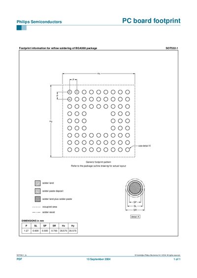
This document supplies the printed‑circuit‑board (PCB) footprint data required for reflow soldering of the Philips SOT532-1 BGA388 package. It includes the layout of solder lands, solder paste deposits, and the overall occupied area.
The key dimensions are listed in millimetres, covering pad pitch, solder land size, solder resist area and overall footprint extents. Refer to the package outline drawing for the exact layout.
| Pad pitch (P) | 1.27 mm |
|---|---|
| Solder land width (SL) | 0.600 mm |
| Solder land length (sP) | 0.500 mm |
| Solder resist width (SR) | 0.750 mm |
| Footprint width (Hx) | 35.575 mm |
| Footprint height (Hy) | 35.575 mm |
The pad pitch (P) is 1.27 mm.
The footprint measures 35.575 mm in width (Hx) and 35.575 mm in height (Hy).