
This document provides information about the dimensions of the SOT570-1 PC board. It includes soldering dimensions and solder pad information for the TFBGA180 package.
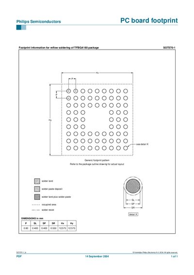
This document describes the recommended PCB footprint for the Philips SOT570-1 TFBGA180 semiconductor package, including solder land definitions and paste deposit guidelines for reflow soldering.
It lists the exact pad dimensions, spacing, and overall occupied area, and refers to the package outline drawing for the complete layout.
The footprint dimensions are P=0.80 mm, SL=0.400 mm, sP=0.400 mm, SR=0.550 mm, Hx=12.575 mm, Hy=12.575 mm.
It was published on 14 September 2004.