
This document is a description of the PCB printed circuit board footprint dimensions for SOT631-1
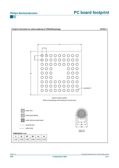
This document supplies the PCB footprint information required for reflow soldering of the Philips SOT631-1 LFBGA208 package. It includes the generic footprint pattern and recommended solder land and paste deposit areas.
The listed dimensions (pitch, solder land size, and pad heights) are given in millimetres and should be used when designing the board layout. Refer to the package outline drawing for the actual layout details.
| Pitch (P) | 0.80 mm |
|---|---|
| Solder land (SL) | 0.330 mm |
| sP | 0.400 mm |
| SR | 0.480 mm |
| Height X (Hx) | 15.575 mm |
| Height Y (Hy) | 15.575 mm |
The document provides a generic footprint pattern that should be used for the SOT631-1 LFBGA208 package.
The footprint dimensions are Pitch 0.80 mm, Solder land 0.330 mm, sP 0.400 mm, SR 0.480 mm, Height X 15.575 mm, and Height Y 15.575 mm.