
SOT635-1_fp PDF file is a printed circuit board silk screen drawing released by Philips Semiconductors about SOT635-1 package. The drawing lists the details of the package dimensions, pad sizes, solder paste sizes, etc.
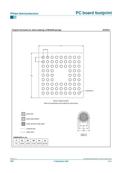
This document describes the PCB footprint for the Philips SOT635-1 (HBGA596) semiconductor package, including solder land and paste deposit guidelines for reflow soldering.
It lists the exact dimensions of the generic footprint pattern and refers to the package outline drawing for the final layout.
| P (mm) | 1.27 |
|---|---|
| SL (mm) | 0.600 |
| sP (mm) | 0.500 |
| SR (mm) | 0.750 |
| Hx (mm) | 40.575 |
| Hy (mm) | 40.575 |
The pad pitch is 1.27 mm.
The solder land dimensions are SL 0.600 mm, sP 0.500 mm, and SR 0.750 mm.