
This document introduces the dimensions, occupied area, and package information of SOT320-3.
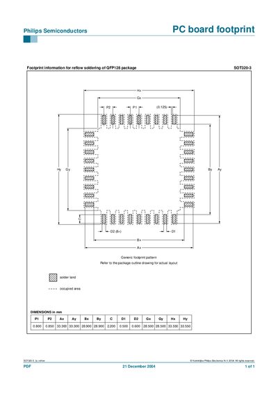
This document supplies the recommended PCB footprint for the Philips SOT320-3 semiconductor package, intended for use in reflow soldering processes. It includes the generic footprint pattern and the exact dimensions of pads and land areas.
The footprint data are presented in millimetres, with pad width, length, pitch and overall dimensions listed. Users should refer to the package outline drawing for the final layout and verify that the occupied area matches the design rules.
| Pad width (Px) | 0.800 mm |
|---|---|
| Pad length (Py) | 0.850 mm |
| Pad pitch (Cx) | 33.300 mm |
| Pad pitch (Cy) | 33.300 mm |
The pad width (Px) is specified as 0.800 mm.
Refer to the generic footprint pattern shown in the document and the package outline drawing for the full layout.