
The XC62G series are highly precise, low power consumption positive voltage regulators, manufactured using CMOS and laser trimming technologies. The series achieves high output currents, with low input- output voltage differentials, and consists of a high precision voltage reference, an error amplifier and power MOSFET, suitable for applications such as battery-powered equipment, cellular phone supplies, cameras, video recorders and palmtops.
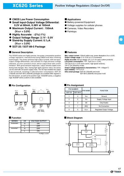
The XC62G series are positive voltage regulators built with CMOS and laser‑trimming technology. They provide precise output voltages, low input‑output differential, and include an error‑correction circuit and a current‑limited output driver. Available in SOT‑25 (150 mW) and SOT‑89‑5 (500 mW) packages, they are suited for battery‑powered equipment, cellular phone supplies, cameras, and palmtops.
The document lists pin assignments, electrical characteristics, marking codes, and a range of performance graphs such as output voltage versus load current, CE pin threshold voltage, supply current versus input voltage, and transient response curves. Detailed specifications cover output voltage range, maximum output current, standby supply current, and ripple rejection. This manual is written in Chinese.
| Maximum Output Current | 150 mA (VOUT = 3.0 V) |
|---|---|
| Output Voltage Range | 2.1 V – 5.0 V |
| Stand‑by Supply Current | 0.1 µA (VOUT = 3.0 V) |
| Typical Supply Current | 13 µA (VOUT = 3.0 V) |
The regulators can deliver up to 150 mA at a 3.0 V output.
It supports output voltages from 2.1 V to 5.0 V in 0.1 V steps.
The standby current is only 0.1 µA when the output is 3.0 V.
The device is offered in SOT‑25 (150 mW) and SOT‑89‑5 (500 mW) packages.