
Key facts
- Model
- LMV844
- Industry
- Industrial
- Documents
- 2
- Languages
- EN
- Last added
- 2012-05-04
Start here
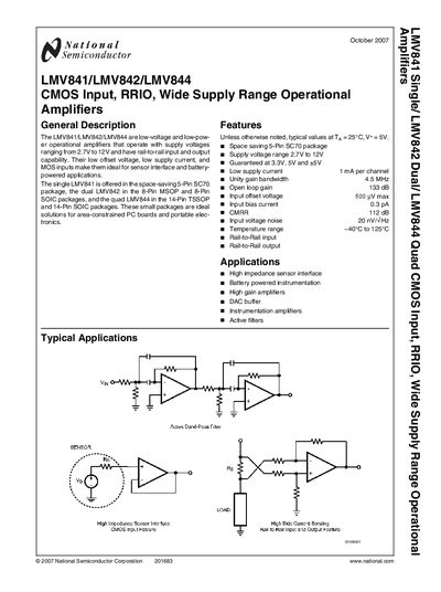
National Semiconductor LMV841/LMV842/LMV844 Datasheet
The LMV841 (single), LMV842 (dual) and LMV844 (quad) are CMOS input, rail‑to‑rail I/O operational amplifiers offered in compact 5‑Pin SC70, 8‑Pin MSOP/SOIC and 14‑Pin TSSOP/SOIC packages. They operate from 2.7 V to 12 V, making them suitable for high‑impedance sensor interfaces, battery‑powered instrumentation, DAC buffers, and active filters.
Key electrical characteristics include low supply current (≈1 mA per channel), input offset voltage as low as 50 µV typical, input bias current of 0.3 pA typical, unity‑gain bandwidth of 45 MHz, and CMRR up to 112 dB. Ordering information and package markings are provided for each device variant.
National Semiconductor LMV844 specifications
| Supply voltage range | 2.7 V to 12 V |
|---|---|
| Supply current per channel | ≈1 mA |
| Input offset voltage (typical) | 50 µV |
| Input bias current (typical) | 0.3 pA |
| Gain bandwidth product | 45 MHz |
Source: National Semiconductor LMV841/LMV842/LMV844 Datasheet
All National Semiconductor LMV844 documents by type
Ratings, dimensions and ordering codes, for selection and design work.
Questions answered in these manuals
What is the supply voltage range for the LMV841/LMV842/LMV844?
The devices operate from 2.7 V up to 12 V.
What is the typical input offset voltage?
Typical input offset voltage is 50 µV.
What supply voltage range do the LMV841 and LMV844 support?
Both devices operate with a supply voltage from 2.7 V up to 12 V.
What is the input offset voltage specification?
The input offset voltage is specified as 500 pV maximum.