
This document describes the features and characteristics of the Altera MAX 3000A programmable logic device family, including high performance, low cost, EEPROM-based architecture, 3.3V in-system programmability, built-in JTAG interface, boundary-scan test, etc.
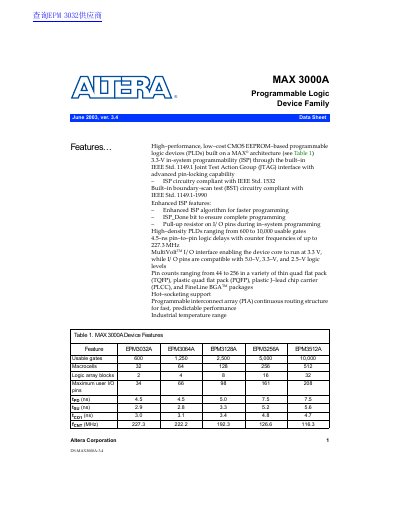
The document describes the MAX 3000A family of programmable logic devices (PLDs), which are high-performance, low-cost CMOS EEPROM-based devices built on the MAX architecture. These devices offer in-system programmability (ISP) via IEEE Std. 1149.1 JTAG interface and support a wide range of pin counts and packages, including TQFP, PQFP, PLCC, and FineLine BGA.
Key features include high-density logic ranging from 600 to 10,000 usable gates, pin-to-pin logic delays as fast as 4.5 ns, and counter frequencies up to 227.3 MHz. The architecture supports MultiVolt I/O interfaces, allowing the device core to run at 3.3 V while I/O pins are compatible with 5.0 V, 3.3 V, and 2.5 V logic levels. The datasheet also covers device speed grades, macrocell configurations, and compatibility with PCI specifications.
| Usable gates | 600 to 10,000 |
|---|---|
| Pin-to-pin logic delays | 4.5 ns |
| Counter frequencies | up to 227.3 MHz |
| Supply voltage | 3.3 V |
| I/O voltage compatibility | 5.0 V, 3.3 V, and 2.5 V |
| Programming cycles | up to 100 times |
| Macrocells per device | 32 to 512 |
The maximum counter frequency is up to 227.3 MHz.
Yes, they support 3.3-V in-system programmability (ISP) through the JTAG interface.
The I/O pins are compatible with 5.0-V, 3.3-V, and 2.5-V logic levels.