
This document describes the pin-out of the EPM3512A chip. The EPM3512A is a chip with 208-pin PQFP package and 256-pin FineLine BGA package. The document provides information about the functions and connections of different pins.
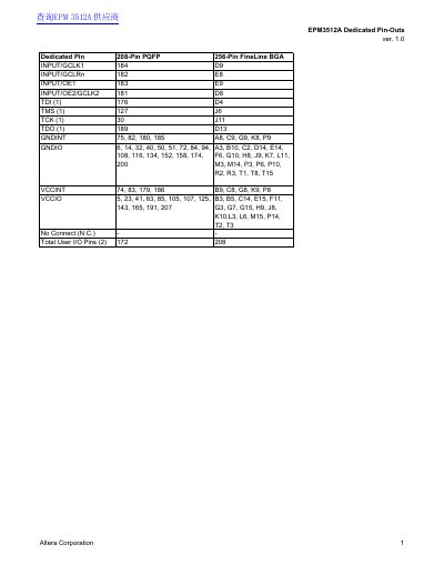
This document details the dedicated pin assignments for the Altera EPM3512A programmable logic device. It covers specific functions such as JTAG inputs (TDI, TMS, TCK, TDO), global clock inputs (GCLK1, GCLK2), and output enable pins (OE1, OE2). The pinout is provided for both the 208-Pin PQFP and 256-Pin FineLine BGA package types.
| Package Types | 208-Pin PQFP, 256-Pin FineLine BGA |
|---|---|
| Total User I/O Pins | 172 |
The JTAG port pins are TDI, TMS, TCK, and TDO.
The output enable pins are INPUT/OE1 and INPUT/OE2.
Yes, but they are not available as user I/O pins when the device is configured for in-system programming.