
Altera EPM3128A Dedicated Pin-Outs Datasheet

This is the pin-out information of EPM3128A.

Altera EPM3128A Dedicated Pin-Outs Datasheet - cover page
Brand
Altera
Category
Other Electronics
Document type
Datasheet
Language
English
Pages
6
File format
PDF
File size
36 KB
Published
06 August, 2012
Updated
30 September, 2023
MD5 checksum
BDCF29046F8A710F285901D61B18D4BC

About this manual

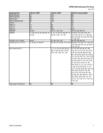
This document provides a comprehensive list of dedicated input pins and I/O pin locations for the Altera EPM3128A device. It covers three specific package types: 100-Pin TQFP, 144-Pin TQFP, and 256-Pin FineLine BGA.

The datasheet includes a summary table of dedicated functions such as JTAG ports (TDI, TMS, TCK, TDO), clock inputs, and output enables. It also provides detailed pin-by-pin tables mapping each logic cell to its physical location on the package for all three form factors.

What's inside

  • Dedicated Pin-Outs
  • I/O Pin-Outs
  • Package Types
  • JTAG Port Pins
  • Power and Ground Pins
  • No Connect (N.C.) Pins
  • Pin Count Summary
  • Notes on Functionality

Frequently asked questions

What are the available package types for the EPM3128A?

The device is available in 100-Pin TQFP, 144-Pin TQFP, and 256-Pin FineLine BGA packages.

Can JTAG port pins be used as user I/O pins?

Yes, these pins may function as either a JTAG port or a user I/O pin depending on configuration.

Download PDF (36 KB)

More Altera Manuals


View all Altera manuals →