
The CycloneTM field programmable gate array family is based on a 1.5-V, 0.13-µm, all-layer copper SRAM process, with densities up to 20,060 logic elements (LEs) and up to 288 Kbits of RAM. It features PLLs for clocking and a dedicated DDR interface for memory requirements. Cyclone devices are cost-effective for data-path applications and support various I/O standards including LVDS and PCI. Low-cost serial configuration devices are available for configuring Cyclone devices.
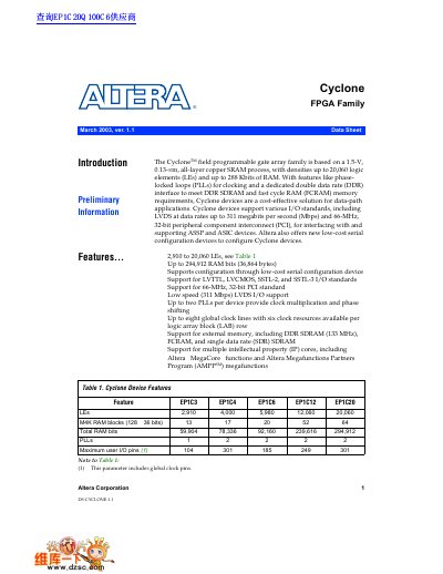
This document is a preliminary data sheet for the Altera Cyclone™ field programmable gate array (FPGA) family, released in March 2003. The Cyclone family is based on a 1.5-V, 0.13-µm SRAM process and includes devices with logic element densities ranging from 2,910 to 20,060 LEs. Key features include embedded M4K RAM blocks, phase-locked loops (PLLs), and support for various I/O standards such as LVDS, PCI, and DDR SDRAM interfaces.
| Logic Elements (LEs) | 2,910 to 20,060 |
|---|---|
| RAM Capacity | Up to 288 Kbits |
| Process Technology | 1.5-V, 0.13-µm SRAM |
| Maximum LVDS Data Rate | 311 Mbps |
| PCI Support | 66-MHz, 32-bit |
| PLL Count | Up to 2 per device |
| Global Clock Lines | 8 |
Cyclone devices are based on a 1.5-V, 0.13-µm, all-layer copper SRAM process.
The Cyclone family has densities up to 20,060 logic elements (LEs).
Cyclone devices are supported by the Altera Quartus II design software.