
The FQD13N06 / FQU13N06 is a N-Channel enhancement mode power field effect transistor produced using Fairchild’s proprietary, planar stripe, DMOS technology. This advanced technology has been especially tailored to minimize on-state resistance, provide superior switching performance, and withstand high energy pulse in the avalanche and commutation mode. These devices are well suited for low voltage applications such as DC/DC converters, high efficiency switching for power management in portable and battery operated products.
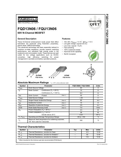
This document is a datasheet for the Fairchild Semiconductor FQD13N06 and FQU13N06 N-Channel enhancement mode power field effect transistors. These devices utilize the company's proprietary planar stripe, DMOS technology to minimize on-state resistance and provide superior switching performance. They are designed for low voltage applications such as DC/DC converters and power management in portable products.
| Drain-Source Voltage | 60 V |
|---|---|
| Continuous Drain Current (Tj = 25°C) | 10 A |
| Continuous Drain Current (Tj = 100°C) | 6.3 A |
| Pulsed Drain Current | 40 A |
| Gate-Source Voltage | -25 to +25 V |
| On-Resistance (Vgs = 10V, Id = 5.0A) | 0.11 to 0.14 Ohm |
| Total Gate Charge | 5.8 to 75 nC |
| Operating Temperature Range | -55 to +150 °C |
| Package Types | D-PAK, I-PAK |
The maximum continuous drain current at a junction temperature of 25°C is 10 A.
The static drain-source on-resistance is typically between 0.11 and 0.14 Ohms when Vgs is 10V and Id is 5.0A.
The device is available in D-PAK and I-PAK packages.