
The FQA11N90C_F109 is a 900V N-channel MOSFET that features low gate charge (typical 60 nC), low Crss (typical 23pF), fast switching, 100% avalanche tested, improved dv/dt capability, and RoHS compliance.
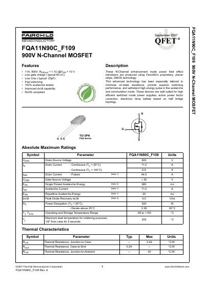
This document is a datasheet for the Fairchild Semiconductor FQA11N90C_F109, a 900V N-Channel enhancement mode power field effect transistor. Produced using proprietary planar stripe DMOS technology, the device is designed for high efficiency switched mode power supplies, active power factor correction, and electronic lamp ballasts. Key features include a typical on-state resistance of 1.12 ohms at VDS=10V, low gate charge of 60 nC, and fast switching capabilities.
| Drain-Source Voltage | 900 V |
|---|---|
| Continuous Drain Current (Tj=25°C) | 11.0 A |
| Continuous Drain Current (Tj=100°C) | 6.9 A |
| Pulsed Drain Current | 44.0 A |
| Gate-Source Voltage | +30 V |
| Single Pulsed Avalanche Energy | 960 mJ |
| Power Dissipation (Tc=25°C) | 300 W |
| Operating and Storage Temperature Range | -55 to +150 °C |
| Thermal Resistance, Junction-to-Case | 0.42 °C/W |
| Thermal Resistance, Case-to-Sink | 0.24 °C/W |
| Package Type | TO-3PN |
The typical gate charge is 60 nC.
The typical on-state resistance is 1.12 ohms.
Yes, the device is RoHS compliant.
The maximum lead temperature for soldering purposes is 300 °C.