
The FDS6982AS is a device designed to replace two single SO-8 MOSFETs and a Schottky diode in synchronous DC:DC power supplies that provide various peripheral voltages for notebook computers and other battery-powered electronic devices. It contains two unique 30V, N-channel, logic level, PowerTrench MOSFETs designed to maximize power conversion efficiency. The high-side switch (Q1) is designed with specific emphasis on reducing switching losses, while the low-side switch (Q2) is optimized to reduce conduction losses. Q2 also includes an integrated Schottky diode using Fairchild's monolithic SyncFET technology.
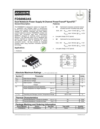
The FDS6982AS is designed to replace two single SO-8 MOSFETs and Schottky diodes in synchronous DC/DC power supplies used in battery-powered electronic devices. It contains two unique 30V, N-channel, logic-level PowerTrench MOSFETs: a high-side switch optimized for low switching losses and a low-side switch with an integrated SyncFET Schottky body diode to minimize conduction losses.
The document provides comprehensive electrical characteristics, including absolute maximum ratings, on/off state parameters, dynamic capacitance, and switching times. It also includes typical performance curves illustrating on-resistance variation with temperature and current, gate charge characteristics, and safe operating areas for both Q1 and Q2 devices.
| Drain-Source Voltage (Q1, Q2) | 30 V |
|---|---|
| On-Resistance (Q2, Vgs=4.5V) | Max 16.5 mΩ |
| On-Resistance (Q1, Vgs=4.5V) | Max 35.0 mΩ |
| Package Type | SO-8 |
Yes, Q2 includes an integrated Schottky body diode using Fairchild's monolithic SyncFET technology.
The maximum power dissipation for dual operation is 2 W.