
FDS6890A is a dual N-channel 2.5V specified MOSFET manufactured by Fairchild Semiconductor. It uses the PowerTrench process and has extremely low RDS(ON) and low gate charge, which enables fast switching speed and high power and current handling capability.
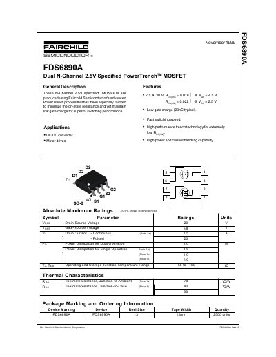
This document is a technical datasheet for the Fairchild Semiconductor FDS6890A, a dual N-Channel MOSFET utilizing the company's advanced PowerTrench process. The device is specifically designed with a 2.5V gate threshold voltage to minimize on-state resistance while maintaining low gate charge for superior switching performance.
The datasheet provides comprehensive electrical characteristics, including absolute maximum ratings, thermal data, and typical operating curves. It details parameters such as drain-source breakdown voltage, static drain-source on-resistance, total gate charge, and capacitance values under various test conditions.
| Drain-Source Voltage (Vdss) | 20 V |
|---|---|
| Gate-Source Voltage (Vgss) | +8 V |
| Pulsed Drain Current (Id) | 20 A |
| Power Dissipation (Dual Operation) | 2.0 W |
| Operating Junction Temperature Range | -55 to +150 °C |
| Total Gate Charge (Qg) | 23 to 32 nC |
| Input Capacitance (Ciss) | 2130 pF |
The device is suitable for use in DC/DC converters and motor drives.
It is a dual N-channel device, with power dissipation ratings provided for both dual and single operation.