
This document describes the features and characteristics of the FDS6911 Dual N-Channel Logic Level PowerTrench MOSFET produced by Fairchild Semiconductor. These devices are well suited for low voltage and battery powered applications where low in-line power loss and fast switching are required.
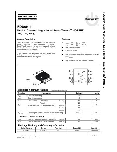
The FDS6911 is a dual N-channel logic level MOSFET produced using Fairchild Semiconductor's advanced PowerTrench process. These devices are designed to minimize on-state resistance while maintaining superior switching performance, making them well-suited for low voltage and battery-powered applications requiring low in-line power loss and fast switching.
| Drain-Source Voltage | 20 V |
|---|---|
| Gate-Source Voltage | +20 V |
| Pulsed Drain Current | 20 A |
| Operating Junction Temperature Range | -55 to +150 °C |
| On-Resistance (Vgs=10V, Id=7.5A) | 13 mΩ |
| Total Gate Charge (Vgs=10V) | 24 nC |
The operating and storage junction temperature range is -55 to +150 °C.
The on-state resistance is 13 mΩ under these conditions.