
This document describes the maximum ratings and static electrical characteristics of the APT10M19SVR model product. The product is a high voltage N-Channel enhancement mode power MOSFET with low on-state resistance and high packing density. The document provides detailed information on the working principle, maximum voltage, maximum current, maximum power, and other characteristics of the product.
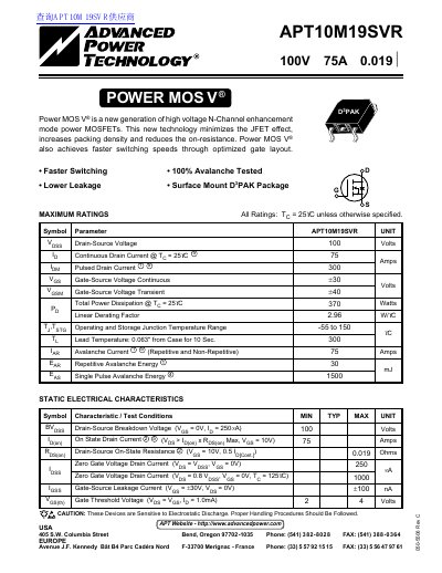
This document provides technical specifications for the Advanced APT10M19SVR, a new generation high voltage N-Channel enhancement mode power MOSFET. The device features minimized JFET effect, increased packing density, and reduced on-resistance, achieving faster switching speeds through optimized gate layout. It is available in a surface mount D°PAK package.
| Drain-Source Voltage | 100 Volts |
|---|---|
| Continuous Drain Current | 75 Amps |
| Pulsed Drain Current | 300 Amps |
| Total Power Dissipation | 370 Watts |
| Operating Junction Temperature Range | -55 to 150 C |
| Drain-Source On-State Resistance | 0.019 Ohms |
| Package Type | D°PAK |
The maximum continuous drain current is 75 Amps at a junction temperature of 25°C.
The typical drain-source on-state resistance is 0.019 Ohms when Vgg is 10V.