
This document describes the maximum ratings, characteristics, and test conditions of the products with model numbers APT10M1LVR and APT10M11LVR. It includes parameters such as drain-source breakdown voltage, on-state drain current, drain-source on-state resistance, zero gate voltage drain current, gate-source leakage current, and gate threshold voltage.
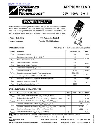
This document provides technical specifications for the APT10M11LVR, a high voltage N-Channel enhancement mode power MOSFET. The device features Power MOS V® technology which minimizes the JFET effect to reduce on-resistance and increase packing density.
Key electrical characteristics include a drain-source breakdown voltage of 100 Volts, a continuous drain current of 100 Amps at 25°C, and an on-state resistance (Rds(on)) of 0.011 Ohms. The datasheet also covers dynamic characteristics such as capacitance values and switching times, along with thermal data for the TO-264 package.
| Drain-Source Voltage (Vdss) | 100 Volts |
|---|---|
| Continuous Drain Current (Id) | 100 Amps |
| On-State Resistance (Rds(on)) | 0.011 Ohms |
| Total Power Dissipation | 520 Watts |
| Operating Junction Temperature Range | -55 to 150 C |
The device supports a continuous drain current of 100 Amps when the temperature is 25°C.
The total power dissipation is rated at 520 Watts when the temperature is 25°C.
The device operates and stores within a junction temperature range of -55 to 150 C.