
This document is the technical information manual for 100V 100A 0.009µF APT10M09B2VR, which mainly introduces the product's maximum ratings, static electrical characteristics, etc.
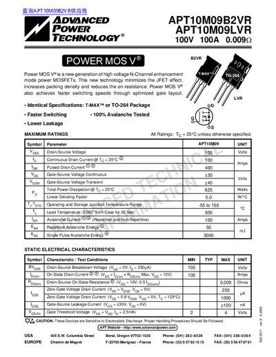
This document provides technical specifications for the Advanced Power Technology APT10M09B2VR and APT10M09LVR, which are new generation high voltage N-Channel enhancement mode power MOSFETs. The devices feature a T-MAX (TO-264) or TO-264 package design intended to minimize the JFET effect, increase packing density, reduce on-resistance, and achieve faster switching speeds through optimized gate layout.
The datasheet details maximum ratings including 100V drain-source voltage and 100A continuous drain current. It also lists static electrical characteristics such as a typical drain-source on-state resistance of 0.009 Ohms, dynamic characteristics like input/output capacitance, and thermal characteristics including junction-to-case resistance.
| Drain-Source Voltage | 100 Volts |
|---|---|
| Continuous Drain Current | 100 Amps |
| Pulsed Drain Current | 400 Amps |
| Drain-Source On-State Resistance | 0.009 Ohms |
| Total Power Dissipation | 625 Watts |
| Operating Junction Temperature Range | -55 to 150 °C |
The device supports a continuous drain current of 100 Amps when the temperature is 25°C.
The MOSFET can dissipate up to 625 Watts when the case temperature is maintained at 25°C.
The device operates within a junction temperature range of -55 to 150 °C.