
This document describes the features and characteristics of the TO-258 model product, including drain-source breakdown voltage, on-state drain current, drain-source on-state resistance, zero gate voltage drain current, etc.
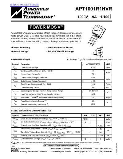
This document is a technical datasheet for the APT1001R1HVR, an N-Channel enhancement mode Power MOS V® device. This new generation of high voltage MOSFETs minimizes the JFET effect and reduces on-resistance while achieving faster switching speeds through optimized gate layout.
The document provides maximum ratings, static electrical characteristics, dynamic characteristics, thermal characteristics, and typical performance curves for the device in a TO-258 package. It includes safe operating area graphs and physical dimensions.
| Drain-Source Voltage | 1000 Volts |
|---|---|
| Continuous Drain Current @ Tg = 25°C | 9 Amps |
| Pulsed Drain Current | 36 Amps |
| Total Power Dissipation @ Tg = 25°C | 200 Watts |
| Operating and Storage Junction Temperature Range | -55 to 150 C |
| Drain-Source On-State Resistance @ Vgg = 10V, Id=0.5A | 1.1 Ohms |
| Package Type | TO-258 |
The maximum continuous drain current is 9 amps when the temperature is 25°C.
The total power dissipation is 200 watts at a temperature of 25°C.
The operating and storage junction temperature range is from -55 to 150 C.