
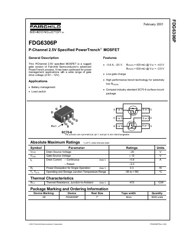
This is the February 2001 Fairchild Semiconductor datasheet (Rev C) for the FDG6306P, a P-channel 2.5V specified PowerTrench MOSFET described as a rugged gate version of Fairchild's advanced PowerTrench process. It is optimized for power management applications with a gate drive voltage range of 2.5V to 12V, and the listed applications are battery management and load switch.
The document gives absolute maximum ratings, thermal characteristics, package marking and ordering information, full electrical characteristics (off, on, dynamic, switching and drain-source diode), and a set of typical characteristic curves including on-region, on-resistance, transfer, gate charge, capacitance, safe operating area and transient thermal response. The device is supplied in a compact industry standard SC70-6 surface mount package with symmetrical pinouts.
| Drain-Source Voltage (V_DSS) | -20 V |
|---|---|
| Gate-Source Voltage (V_GSS) | ±12 V |
| Continuous Drain Current | -0.6 A |
| Pulsed Drain Current | -2.0 A |
| Power Dissipation for Single Operation | 0.3 W |
| Operating and Storage Junction Temperature Range | -55 to +150 °C |
| Thermal Resistance, Junction-to-Ambient | 415 °C/W |
| Input Capacitance (C_iss) | 114 pF |
| Package | SC70-6 surface mount |
It is optimized for power management applications with a wide gate drive voltage range of 2.5V to 12V.
It comes in a compact industry standard SC70-6 surface mount package.
The pinouts are symmetrical, so pin 1 and pin 4 are interchangeable.
The datasheet lists battery management and load switch as applications.