
This document describes the features and characteristics of the FDG6304P Dual P-Channel, Digital FET released in July 1999.
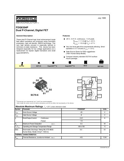
This document describes the Fairchild FDG6304P, a dual P-Channel logic level enhancement mode field effect transistor. The device utilizes proprietary DMOS technology to minimize on-state resistance and is designed specifically for low voltage applications as a replacement for bipolar digital transistors and small signal MOSFETs.
The datasheet provides comprehensive electrical characteristics, including absolute maximum ratings such as a drain-source voltage of -25V and continuous current of 0.41A. It details on-resistance values under various conditions, switching parameters like turn-on delay time, and dynamic characteristics including input and output capacitance.
| Drain-Source Voltage (Vss) | -25 V |
|---|---|
| Gate-Source Voltage (Vgs) | 8 V |
| Continuous Drain/Output Current | 0.41 A |
| Maximum Power Dissipation (Ryax) | 0.3 W |
| Operating and Storage Temperature Range | -55 to 150 C |
| ESD Electrostatic Discharge Rating | 6.0 kV |
| Thermal Resistance, Junction-to-Ambient (Rca) | 415 C/W |
| Static Drain-Source On-Resistance (Vgs=-4.5V) | 0.85 - 1 Ohm |
| Package Type | SC70-6 |
The maximum continuous drain/output current is 0.41 A.
The device is designed for low voltage applications with a gate-source voltage of less than 1.5 V.
No, Fairchild's products are not authorized for use as critical components in life support devices without express written approval.