
The FDG6301N is a dual N-channel digital field effect transistor with a maximum voltage of 25 V and a maximum current of 0.22 A. It features a low threshold voltage, high density process, and compact package, making it ideal for low voltage applications.
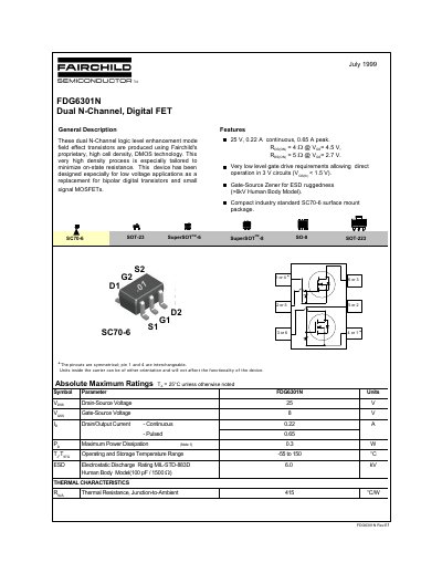
This document is a technical datasheet for the Fairchild Semiconductor FDG6301N, a dual N-Channel logic level enhancement mode field effect transistor. The device utilizes proprietary DMOS technology designed to minimize on-state resistance and is intended as a replacement for bipolar digital transistors and small signal MOSFETs in low voltage applications.
| Drain-Source Voltage (Vss) | 25 V |
|---|---|
| Gate-Source Voltage (Vgs) | 8 V |
| Continuous Drain/Output Current | 0.22 A |
| Pulsed Drain/Output Current | 0.65 A |
| Maximum Power Dissipation | 0.3 W |
| Operating and Storage Temperature Range | -55 to 150 °C |
| ESD Electrostatic Discharge Rating | 6.0 kV Human Body Model |
The device supports a continuous drain current of 0.22 A.
The maximum drain-source voltage is 25 V.
The maximum power dissipation is 0.3 W.