
FDG312P is a P-Channel MOSFET produced by Fairchild Semiconductor using the advanced PowerTrench process. It can achieve low on-state resistance and low gate charge, and is suitable for portable electronic applications.
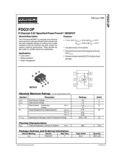
This document is a datasheet for the Fairchild FDG312P, a P-Channel MOSFET produced using the PowerTrench process. It is designed to minimize on-state resistance while maintaining low gate charge, making it suitable for portable electronics applications such as load switches and battery protection. The device is available in a compact industry standard SC70-6 surface mount package.
The datasheet provides comprehensive electrical characteristics, including absolute maximum ratings, thermal characteristics, and typical performance curves. It details parameters such as drain-source voltage, gate threshold voltage, on-resistance, and switching times under various test conditions.
| Drain-Source Voltage | -20 V |
|---|---|
| Gate-Source Voltage | ±8 V |
| Continuous Drain Current | -1.2 A |
| Power Dissipation (Single Operation) | 0.75 W |
| Operating Junction Temperature Range | -55 to +150 °C |
| Thermal Resistance (Junction-to-Ambient) | 260 °C/W |
| Package Type | SC70-6 |
| Gate Charge (Typical) | 3.3 nC |
The maximum continuous drain current is -1.2 A.
The maximum drain-source voltage is -20 V.
The typical total gate charge is 3.3 nC.