
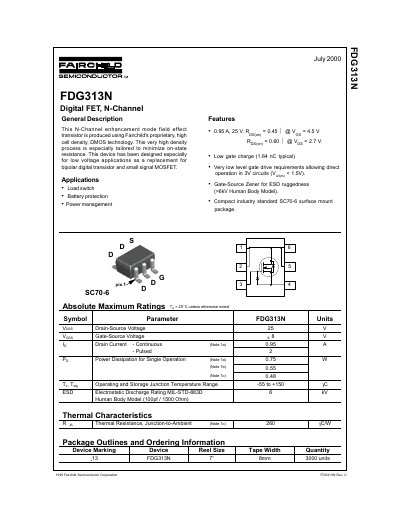
The FDG313N is an N-channel enhancement mode field effect transistor produced with Fairchild's DMOS technology. The datasheet describes it as intended for low-voltage applications as a replacement for bipolar digital transistors and small-signal MOSFETs, with applications including load switching, battery protection, and power management.
The document provides absolute maximum ratings, thermal characteristics, electrical characteristics, typical performance curves, and package outlines and ordering information. It also includes trademark, disclaimer, life support policy, and product status definitions.
| Drain-Source Voltage | 25 V |
|---|---|
| Continuous Drain Current | 0.95 A |
| Power Dissipation for Single Operation | 0.75 W |
| Static Drain-Source On-Resistance | 0.45 Ω max at VGS = 4.5 V |
| Total Gate Charge | 1.64 nC typical |
| Electrostatic Discharge Rating | 6 kV |
| Package | SC70-6 surface mount |
| Thermal Resistance, Junction-to-Ambient | 260 °C/W |
The listed applications are load switch, battery protection, and power management.
It uses a compact industry standard SC70-6 surface mount package.
The typical gate charge is 1.64 nC.
The drain-source voltage rating is 25 V.