
This document introduces the FDD3680 N-Channel PowerTrench MOSFET, which is designed specifically to improve the overall efficiency of DC/DC converters. It features faster switching speed and lower gate charge than other MOSFETs with comparable RDS(ON) specifications, making it easier and safer to drive (even at very high frequencies). By using this MOSFET, DC/DC power supply designs with higher overall efficiency can be achieved.
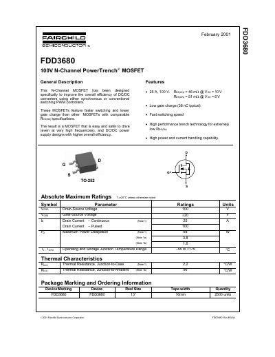
This document is a technical datasheet for the Fairchild Semiconductor FDD3680, an N-Channel MOSFET utilizing PowerTrench technology. The device is specifically designed to enhance the overall efficiency of DC/DC converters by offering faster switching speeds and lower gate charge compared to comparable devices with similar on-resistance specifications.
The datasheet provides comprehensive electrical characteristics, including absolute maximum ratings for voltage and current, thermal resistance values, and dynamic parameters such as input capacitance and total gate charge. It also includes typical performance curves illustrating on-resistance variation with temperature and drain current, as well as safe operating area limits.
| Drain-Source Voltage | 100 V |
|---|---|
| Continuous Drain Current | 25 A |
| Pulsed Drain Current | 100 A |
| Maximum Power Dissipation | 68 W |
| Operating Junction Temperature Range | -55 to +175 °C |
| Thermal Resistance (Junction-to-Case) | 2.2 °C/W |
| Total Gate Charge | 38 nC typical |
This device improves the efficiency of DC/DC converters that use either synchronous or conventional switching PWM controllers.
The device supports a continuous drain current of 25 A.
The typical total gate charge is 38 nC.