
This data sheet is about R6015FNX, which is a high-performance MOSFET with fast reverse recovery time, low on-resistance, fast switching speed, simple drive circuits and easy parallel use.
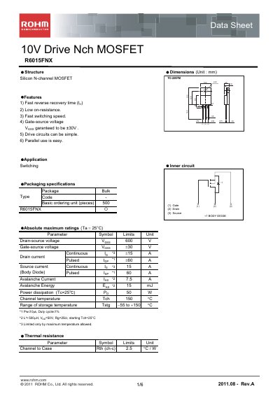
The R6015FNX is a 10 V drive N‑channel MOSFET offered in a TO‑220RM package. It features fast reverse recovery, low on‑resistance, and high switching speed, making it suitable for simple drive circuits and parallel use.
The datasheet lists absolute maximum ratings, thermal resistance, and detailed electrical characteristics such as drain‑source voltage, gate‑source voltage, on‑state resistance, and gate charge. It also includes typical output curves, measurement circuit diagrams, and application notes for switching and power‑handling designs.
| Drain‑source voltage (VDS) | 600 V |
|---|---|
| Gate‑source voltage (VGS) | +30 V |
| Continuous drain current (ID) | 3 A |
| Power dissipation (PD) | 50 W |
| Thermal resistance, junction‑to‑case (RθJC) | 2.5 °C/W |
| Total gate charge (Qg) | 42 nC |
The device can withstand up to 600 V drain‑source voltage.
The gate‑source voltage is guaranteed up to +30 V.
It is supplied in a TO‑220RM (silicon N‑channel MOSFET) package.