
This document describes the application of 2SK1167 and 2SK1168 Silicon N-Channel MOS FETs, highlighting their features such as low on-resistance, high speed switching, low drive current, and no secondary breakdown. They are suitable for switching regulators and DC-DC converters.
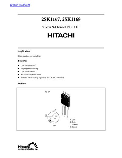
The 2SK1167 and 2SK1168 are silicon N‑channel MOSFETs designed for high‑speed power switching applications such as switching regulators and DC‑DC converters. They feature low on‑resistance, high speed switching, low drive current and no secondary breakdown.
The datasheet lists absolute maximum ratings, detailed electrical characteristics, typical output curves, and thermal performance. It also includes cautions regarding warranty, licensing and proper use within specified limits.
| Drain‑to‑source voltage (VDS) | 450 V (2SK1167) / 500 V (2SK1168) |
|---|---|
| Gate‑to‑source voltage (VGS) | +30 V |
| Drain current (ID) | 15 A |
| Input capacitance (Ciss) | 2050 pF |
| Output capacitance (Coss) | 600 pF |
| Body‑to‑drain diode reverse recovery time | 500 ns |
| Maximum operating temperature | 150 °C |
The 2SK1167 is rated for a maximum drain‑to‑source voltage of 450 V.
The typical on‑state resistance of the 2SK1168 is about 0.30 Ω.
They are intended for high‑speed power switching, switching regulators and DC‑DC converters.
No, Hitachi does not grant licenses for any patents, copyrights or trademarks contained in the document.