
BS616LV2013 is a high performance, very low power CMOS Static Random Access Memory organized as 131,072 words by 16 bits and operates from a wide range of 2.4V to 3.6V supply voltage. Advanced CMOS technology and circuit techniques provide both high speed and low power features with a typical CMOS standby current of 0.1uA and maximum access time of 70/100ns in 3V operation. Easy memory expansion is provided by active LOW chip enable(CE), active LOW output enable(OE) and three-state output drivers. The BS616LV2013 has an automatic power down feature, reducing the power consumption significantly when chip is deselected. The BS616LV2013 is available in DICE form, JEDEC standard 44-pin TSOP Type II package , JEDEC standard 48-pin TSOP Type I package and 48-ball BGA package.
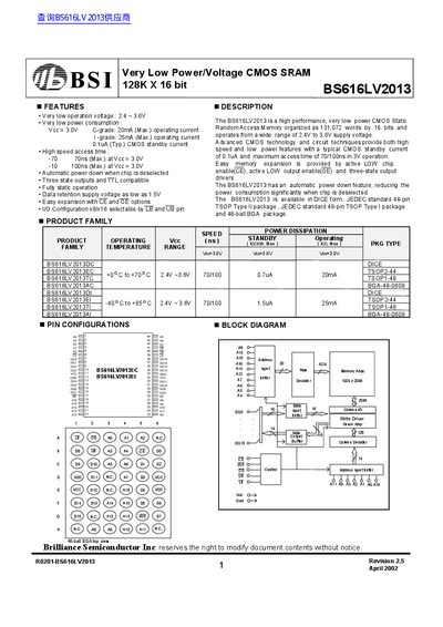
This datasheet describes the BS616LV2013, a 128 K × 16‑bit static RAM built on very‑low‑power CMOS technology. It operates from a wide supply range of 2.4 V to 3.6 V and offers high‑speed access times of 70 ns (typical) or 100 ns at 3.0 V, with a standby current as low as 0.1 µA.
The document includes detailed pin configurations, truth tables, absolute maximum ratings, electrical characteristics, data‑retention behavior, package options (DICE, TSOP‑44, 48‑ball BGA), and ordering information. It also provides timing diagrams for read and write cycles and a revision history.
| Operating voltage range | 2.4 V – 3.6 V |
|---|---|
| CMOS standby current (typical) | 0.1 µA |
| Maximum access time at 3.0 V | 70 ns (typical) / 100 ns (slow) |
| Industrial temperature range | -40 °C to +85 °C |
| Power dissipation | 1.0 W |
| Input low voltage (VIL) | 0.5 V |
| Input high voltage (VIH) | 2.0 V (typical) |
The device operates from 2.4 V up to 3.6 V.
The typical CMOS standby current is 0.1 µA.
The maximum access time is 70 ns (typical) or 100 ns for the slower speed grade.