
The MAX1191 is an ultra-low-power, dual, 8-bit, 7.5Msps analog-to-digital converter (ADC). The device features two fully differential wideband track-and-hold (T/H) inputs. These inputs have a 440MHz bandwidth and accept fully differential or single-ended signals. The MAX1191 delivers a typical signal-to-noise and dis- tortion (SINAD) of 48.6dB at an input frequency of 1.875MHz and a sampling rate of 7.5Msps while con- suming only 12mW. This ADC operates from a 2.7V to 3.6V analog power supply. A separate 1.8V to 3.6V supply powers the digital output driver. In addition to ultra-low operating power, the MAX1191 features three power-down modes to conserve power during idle peri- ods. Excellent dynamic performance, ultra-low power, and small size make the MAX1191 ideal for applica- tions in imaging, instrumentation, and digital communi- cations. An internal 1.024V precision bandgap reference sets the full-scale range of the ADC to ±0.512V. A flexible reference structure allows the MAX1191 to use its inter- nal reference or accept an externally applied reference for applications requiring increased accuracy. The MAX1191 features parallel, multiplexed, CMOS- compatible tri-state outputs. The digital output format is offset binary. A separate digital power input accepts a voltage from 1.8V to 3.6V for flexible interfacing to dif- ferent logic levels. The MAX1191 is available in a 5mm × 5mm, 28-pin thin QFN package, and is specified for the extended industrial (-40°C to 85°C) applications.
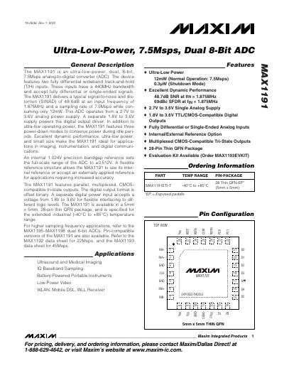
The MAX1191 analog‑to‑digital converter provides two fully differential inputs with a 440 MHz bandwidth and operates from a 2.7 V to 3.6 V analog supply. It features an internal 1.024 V bandgap reference, offset‑binary output format, and tri‑state CMOS‑compatible digital outputs powered by a separate 1.8 V to 3.6 V supply.
Designed for imaging, instrumentation and low‑power communications, the device delivers 48.6 dB SINAD at 7.5 Msps while consuming only 12 mW. It is supplied in a 5 mm × 5 mm, 28‑pin thin QFN package and operates over an extended industrial temperature range of –40 °C to +85 °C.
| Sampling Rate | 7.5 Msps |
|---|---|
| Power Consumption (Normal) | 12 mW |
| Analog Supply Voltage | 2.7 V – 3.6 V |
| Digital Supply Voltage | 1.8 V – 3.6V |
| Input Bandwidth | 440 MHz |
| Resolution | 8 bits |
| SINAD | 48.6 dB |
| Operating Temperature Range | -40 °C to +85 °C |
The device consumes only 12 mW in normal operation.
The analog section runs from 2.7 V to 3.6 V, while the digital output driver uses a separate 1.8 V to 3.6 V supply.
Both inputs have a 440 MHz bandwidth.
The MAX1191 can sample at up to 7.5 Msps.