
The MAX1198 is a 3.3V, dual, 8-bit analog-to-digital converter (ADC) featuring fully differential wideband track- and-hold (T/H) inputs, driving two ADCs. The MAX1198 is optimized for low power, small size, and high-dynamic performance for applications in imaging, instrumenta- tion, and digital communications. This ADC operates from a single 2.7V to 3.6V supply, consuming only 264mW, while delivering a typical signal-to-noise and distortion (SINAD) of 48.1dB at an input frequency of 50MHz and a sampling rate of 100Msps. The T/H-driven input stages incorporate 400MHz (-3dB) input ampli- fiers. The converters may also be operated with single- ended inputs. In addition to low operating power, the MAX1198 features a 3.2mA sleep mode, as well as a 0.15µA power-down mode to conserve power during idle periods. An internal 2.048V precision bandgap reference sets the full-scale range of the ADC. A flexible reference structure allows the use of this internal or an externally applied reference, if desired, for applications requiring increased accuracy or a different input voltage range. The MAX1198 features parallel, CMOS-compatible three- state outputs. The digital output format can be set to two’s complement or straight offset binary through a single con- trol pin. The device provides for a separate output power supply of 1.7V to 3.6V for flexible interfacing with various logic families. The MAX1198 is available in a 7mm x 7mm, 48-pin TQFP package, and is specifi- ed for automotive and industrial applications.
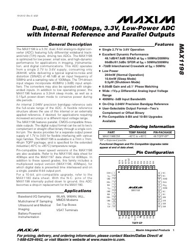
The MAX1198 is a 3.3 V, dual‑channel, 8‑bit analog‑to‑digital converter optimized for low power, small size, and high‑dynamic performance. It supports fully differential wideband track‑and‑hold inputs and can also operate with single‑ended inputs. The device includes an internal 2.048 V precision bandgap reference and selectable output format (two’s complement or offset binary).
Key features include a 100 Msps sampling rate, 264 mW normal‑operation power consumption, sleep mode current of 3.2 mA, shutdown mode current of 0.15 µA, 400 MHz input bandwidth, and operation over an extended temperature range of –40 °C to +85 °C. The ADC is supplied in a 48‑pin TQFP package and offers parallel CMOS‑compatible three‑state outputs.
| Supply Voltage Range | 2.7 V to 3.6 V |
|---|---|
| Sampling Rate | 100 Msps |
| Resolution | 8 bits |
| Normal‑Mode Power Consumption | 264 mW |
| Sleep‑Mode Current | 3.2 mA |
| Shutdown‑Mode Current | 0.15 µA |
| Input Bandwidth (‑3 dB) | 400 MHz |
| Operating Temperature Range | –40 °C to +85 °C |
| Reference Voltage | 2.048 V internal bandgap |
The MAX1198 can sample at up to 100 Msps.
In normal operation the device consumes 264 mW.
It includes an internal 2.048 V precision bandgap reference.