
The MAX1127 is a quad, 12-bit analog-to-digital converter (ADC) with fully differential inputs, a pipelined architecture, and digital error correction. This ADC is optimized for low-power, high-dynamic performance for medical imaging, communications, and instrumentation applications. It operates from a 1.7V to 1.9V single supply and consumes only 563mW while delivering a 69.6dB signal-to-noise ratio (SNR) at a 19.3MHz input frequency. In addition to low operating power, it features a 675µA power-down mode for idle periods. An internal 1.24V precision bandgap reference sets the ADC’s full-scale range. A flexible reference structure allows the use of an external reference for applications requiring increased accuracy or a different input voltage range. A single-ended clock controls the conversion process. An internal duty-cycle equalizer allows for wide variations in input-clock duty cycle. An on-chip phase-locked loop (PLL) generates the high-speed serial low-voltage differential signaling (LVDS) clock. The MAX1127 provides serial LVDS outputs for data, clock, and frame alignment signals. The output data is presented in two’s complement or binary format. Refer to the MAX1126 data sheet for a pin-compatible 40Msps version of the MAX1127. It is available in a small, 10mm x 10mm x 0.9mm, 68-pin QFN package with exposed paddle and is specified for the extended industrial (-40°C to +85°C) temperature range.
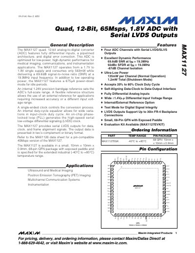
The MAX1127 is a 12‑bit, four‑channel analog‑to‑digital converter featuring fully differential inputs, a pipelined architecture, and digital error correction. It operates from a 1.7 V to 1.9 V single supply and provides serial LVDS outputs in two’s complement or binary format. The device is offered in a compact 68‑pin QFN package and is specified for an extended industrial temperature range.
Key specifications include a maximum conversion rate of 65 MHz, 69.6 dB SNR at 19.3 MHz input, 563 mW power consumption in normal mode, and a low‑power 675 µA shutdown mode. The MAX1127 is suited for ultrasound, PET imaging, multichannel communication systems, and other high‑performance instrumentation applications.
| Resolution | 12 bits |
|---|---|
| Supply Voltage | 1.7 V to 1.9 V |
| Power Consumption (normal) | 563 mW |
| Power‑down Current | 675 µA |
| Signal‑to‑Noise Ratio | 69.6 dB at 19.3 MHz |
| Maximum Conversion Rate | 65 MHz |
| Package | 68‑pin QFN 10 mm × 10 mm × 0.9 mm |
| Differential Input Range | ±1.4 V pp |
| Internal Reference Voltage | 1.24 V |
The MAX1127 operates from a single supply voltage of 1.7 V to 1.9 V.
The device can convert at up to 65 MHz.
It consumes only 563 mW while delivering full performance.
It provides serial LVDS outputs that can be formatted as two’s complement or binary.