
The MAX1193 is an ultra-low-power, dual, 8-bit, 45Msps analog-to-digital converter (ADC). The device features two fully differential wideband track-and-hold (T/H) inputs. These inputs have a 440MHz bandwidth and accept fully differential or single-ended signals. The MAX1193 delivers a typical signal-to-noise and dis- tortion (SINAD) of 48.5dB at an input frequency of 5.5MHz and a sampling rate of 45Msps while consum- ing only 57mW. This ADC operates from a 2.7V to 3.6V analog power supply. A separate 1.8V to 3.6V supply powers the digital output driver. In addition to ultra-low operating power, the MAX1193 features three power- down modes to conserve power during idle periods. Excellent dynamic performance, ultra-low power, and small size make the MAX1193 ideal for applications in imaging, instrumentation, and digital communications. An internal 1.024V precision bandgap reference sets the full-scale range of the ADC to ±0.512V. A flexible reference structure allows the MAX1193 to use its inter- nal reference or accept an externally applied reference for applications requiring increased accuracy. The MAX1193 features parallel, multiplexed, CMOS- compatible tri-state outputs. The digital output format is offset binary. A separate digital power input accepts a voltage from 1.8V to 3.6V for flexible interfacing to dif- ferent logic levels. The MAX1193 is available in a 5mm × 5mm, 28-pin thin QFN package, and is specified for the extended industrial (-40°C to +
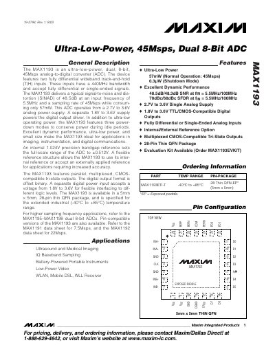
The Maxim MAX1193 is an ultra‑low‑power, dual‑channel 8‑bit analog‑to‑digital converter that samples at up to 45 Msps. It features fully differential wideband track‑and‑hold inputs with 440 MHz bandwidth and operates from a 2.7 V to 3.6 V analog supply.
Typical performance includes 57 mW power consumption, 48.5 dB SINAD, and a 71.5 dBc spurious‑free dynamic range. The device is supplied in a 5 mm × 5 mm, 28‑pin thin QFN package and is rated for –40 °C to +85 °C operation, making it suitable for imaging, instrumentation, and portable communication applications.
| Power consumption (normal operation) | 57 mW |
|---|---|
| Analog supply voltage | 2.7 V to 3.6 V |
| Digital output supply voltage | 1.8 V to 3.6 V |
| Bandwidth | 440 MHz |
| Resolution | 8 bits |
| Package | 5 mm × 5 mm, 28‑pin thin QFN |
| Operating temperature range | ‑40 °C to +85 °C |
| SINAD (45 Msps) | 48.5 dB |
The MAX1193 consumes 57 mW while operating at 45 Msps.
It needs an analog supply of 2.7 V to 3.6 V and a separate digital output supply of 1.8 V to 3.6 V.
The device can sample up to 45 Msps.
It is offered in a 5 mm × 5 mm, 28‑pin thin QFN package.