
Continuous Rate 10 Mb/s to 1.25 Gb/s Clock and Data Recovery IC with Integrated Limiting Amp
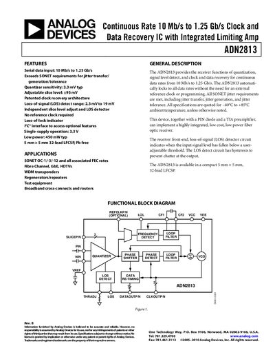
The ADN2813 provides receiver functions for quantization, signal‑level detection, and clock‑and‑data recovery over continuous data rates from 10 Mb/s to 1.25 Gb/s. It operates without an external reference clock, meets SONET jitter requirements, and is supplied in a compact 5 mm × 5 mm 32‑lead LFCSP package.
Key features include a single‑supply 3.3 V operation, low power consumption (≈450 mW), adjustable slice level, loss‑of‑signal detection, and a PC interface for optional features. Detailed specifications cover power, timing, LVDS output, jitter performance, and absolute maximum ratings.
| Data Rate Range | 10 Mb/s to 1.25 Gb/s |
|---|---|
| Supply Voltage | 3.0 V to 3.6 V |
| Supply Current (locked to 1.25 Gb/s) | 139 mA to 155 mA |
| Operating Temperature Range | -40 °C to +85 °C |
| Input Voltage Range (DC‑coupled) | 1.8 V to 2.8 V |
| LVDS Output High Voltage (655 Mb/s) | 1475 mV |
It supports continuous data rates from 10 Mb/s up to 1.25 Gb/s.
The device operates from a single 3.3 V supply, with a recommended range of 3.0 V to 3.6 V.
The ADN2813 is specified for ambient temperatures from –40 °C to +85 °C.