
This datasheet provides detailed information on the 155/622 Mb/s clock and data recovery IC ADN2807, including features, applications, technical specifications, and dimensions.
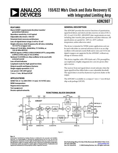
The ADN2807 is a 155/622 Mb/s clock and data recovery IC with integrated limiting amplifier, designed for SONET/SDH applications, WDM transponders, regenerators, test equipment and passive optical networks. It operates from a single 3.3 V supply, offers low power consumption (≈540 mW) and supports multiple reference clock frequencies.
The document provides detailed electrical specifications, absolute maximum ratings, thermal characteristics, pin configuration, functional block diagrams, and ordering information for the 7 mm × 7 mm 48‑lead LFCSP package.
| Power Supply Voltage | 3.0 V (min) – 3.6 V (max) |
|---|---|
| Power Supply Current | 150 mA (min) – 215 mA (max) |
| Input Voltage Range (PIN/NIN) | 0 V – 1.2 V |
| Jitter Transfer Bandwidth (OC‑12) | 140 kHz – 200 kHz |
| Single‑Ended Output Swing | 400 mV (min) – 540 mV (max) |
| Package Size | 7 mm × 7 mm, 48‑lead LFCSP |
The ADN2807 operates from 3.0 V minimum, 3.3 V typical, up to 3.6 V maximum supply voltage.
It is supplied in a 7 mm × 7 mm 48‑lead LFCSP (chip‑scale) package.
The differential inputs (PIN/NIN) accept a dc‑coupled voltage range from 0 V to 1.2 V.