
This document is a datasheet for ADN2817/ADN2818 Continuous Rate 10 Mbps to 2.7 Gbps Clock and Data Recovery ICs. The product features an integrated limiting amplifier, adjustable slice level, patented dual-loop clock recovery architecture, programmable loss of lock detection, integrated PRBS generator and detector, and more.
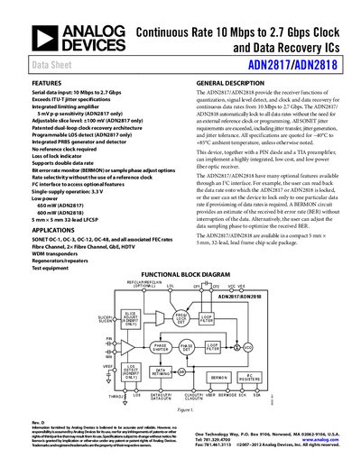
The ADN2817 and ADN2818 are continuous‑rate clock and data recovery ICs that operate from 10 Mbps to 2.7 Gbps without a reference clock. They include an integrated limiting amplifier, programmable loss‑of‑signal detection, PRBS generator/detector, and optional PC‑interface features such as data‑rate readback and slice‑level adjustment.
The devices are supplied in a 5 mm × 5 mm 32‑lead LFCSP, run from a single 3.3 V supply, and consume up to 650 mW (ADN2817) or 600 mW (ADN2818). Detailed electrical specifications, jitter performance, output timing, and BER monitoring parameters are listed in the handbook.
| Data Rate | 10 Mbps to 2.7 Gbps |
|---|---|
| Supply Voltage | 3.3 V (single‑supply) |
| Power Consumption (typical) | 650 mW (ADN2817) / 600 mW (ADN2818) |
| Package | 5 mm × 5 mm 32‑lead LFCSP |
| Input Sensitivity (ADN2817) | 5 mV p‑p |
| Operating Temperature Range | –40 °C to +85 °C |
| Supply Current (ADN2817) | 210‑247 mA |
| Jitter Transfer Bandwidth (OC‑48) | 548‑839 kHz |
| BERMON Input BER Range | 1 × 10³ to 1 × 10⁷ |
The devices accept serial data from 10 Mbps up to 2.7 Gbps.
Both parts operate from a single 3.3 V supply.
Typical power consumption is 650 mW for the ADN2817.
They are available in a 5 mm × 5 mm 32‑lead LFCSP package.