
The ADN2855 is a burst mode clock and data recovery IC designed for GPON/BPON/GEPON optical line terminal (OLT) receiver applications. The device can operate at 155.52 Mbps, 622.08 Mbps, 1244.16 Mbps or 1250.00 Mbps serial data input. It features 12-bit acquisition time, 4-bit parallel LVDS output interface, patented dual-loop clock recovery architecture, integrated PRBS generator, byte rate reference clock, loss-of-lock indicator, supports double data rate (DDR)-compatible FPGA I2C interface to access optional features and single-supply operation (3.3 V).
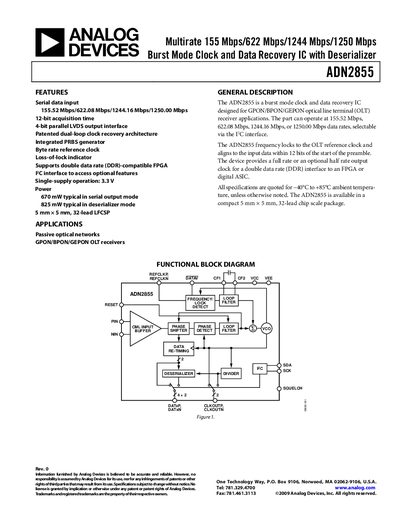
The ADN2855 is a burst mode clock and data recovery IC designed for GPON/BPON/GEPON optical line terminal (OLT) receiver applications. It operates at selectable data rates of 155.52, 622.08, 1244.16 or 1250.00 Mbps, provides a dual‑loop clock recovery architecture, and offers both full‑rate and optional half‑rate output clocks for DDR interfaces.
The device is supplied in a compact 5 mm × 5 mm, 32‑lead LFCSP package, requires a single 3.3 V supply, and consumes up to 825 mW in deserializer mode. It includes a PC interface for optional feature access, a loss‑of‑lock indicator, and an integrated PRBS generator. Operating temperature range is –40 °C to +85 °C.
| Supply voltage | 3.0 V – 3.6 V |
|---|---|
| Typical power consumption (serial output mode) | 670 mW |
| Typical power consumption (deserializer mode) | 825 mW |
| Package | 5 mm × 5 mm, 32‑lead LFCSP |
| Operating temperature range | –40 °C to +85 °C |
| Differential output swing | 260 mV – 400 mV |
| LVDS output rise time (20%‑80%) | 115 ps – 220 ps |
| LVDS output fall time (80%‑20%) | 115 ps – 220 ps |
| Maximum junction temperature | 125 °C |
The typical power consumption is 670 mW in serial output mode.
It is offered in a 5 mm × 5 mm, 32‑lead LFCSP package.
The device operates from –40 °C to +85 °C.