
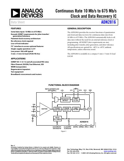
The ADN2816 is a continuous‑rate clock and data recovery IC that operates from 10 Mb/s to 675 Mb/s without an external reference clock. It provides loss‑of‑lock indication, I2C programmable features, and low‑power single‑supply operation.
The document includes sections on features, applications, functional block diagram, detailed specifications, pin configuration, I2C interface timing, jitter performance, and ordering information, allowing designers to integrate the device into SONET, Fibre Channel, Ethernet, and test equipment designs.
| Data Rate Range | 10 Mb/s to 675 Mb/s |
|---|---|
| Supply Voltage | 3.0 V to 3.6 V |
| Operating Temperature Range | −40 °C to +85 °C |
| I2C Clock Frequency | 400 kHz |
| Package | 32‑lead LFCSP, 5 mm × 5 mm |
The differential input pins accept a voltage range of 1.8 V to 2.8 V.
The loss‑of‑lock response time is 4 ms at a 10 Mb/s data rate.
The I2C interface operates with a clock frequency up to 400 kHz.
It is supplied in a 32‑lead LFCSP package measuring 5 mm × 5 mm.