
ADN2812 is a continuous rate 12.3 Mb/s to 2.7 Gb/s clock and data recovery IC with integrated limiting amp
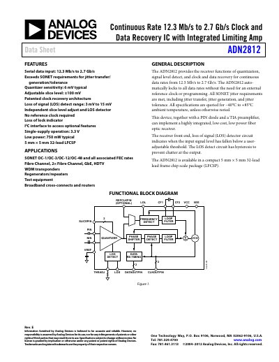
The ADN2812 provides clock and data recovery for continuous data rates from 12.3 Mb/s up to 2.7 Gb/s. It automatically locks without an external reference clock and meets SONET jitter requirements, offering adjustable slice level and loss‑of‑signal detection.
The device is supplied in a 5 mm × 5 mm 32‑lead LFCSP package, operates from a single 3.3 V supply, and includes an I2C interface for optional feature access. It is intended for applications such as SONET, Fibre Channel, GbE, HDTV, and test equipment.
| Data Rate Range | 12.3 Mb/s to 2.7 Gb/s |
|---|---|
| Power Supply Voltage | 3.0 V – 3.6 V (typical 3.3 V) |
| Power Supply Current | 259 mA (typical 235 mA) |
| Operating Temperature Range | –40 °C to +85 °C |
| Input Voltage Range (PIN/NIN) | 1.8 V – 2.8 V |
| Single‑Ended Output Swing (VSE) | 300 mV – 600 mV |
| Loss‑of‑Signal Detect Range | 3 mV – 15 mV |
| I2C Clock Frequency | 400 kHz |
It supports continuous data rates from 12.3 Mb/s up to 2.7 Gb/s.
The device operates from 3.0 V to 3.6 V, with a typical value of 3.3 V.
It is rated for operation from –40 °C to +85 °C.
Yes, it includes an I2C interface with a 400 kHz clock.