
ADN2819 is a high performance multirate clock and data recovery IC with integrated limiting amp, supporting up to 2.7Gb/s bandwidth.
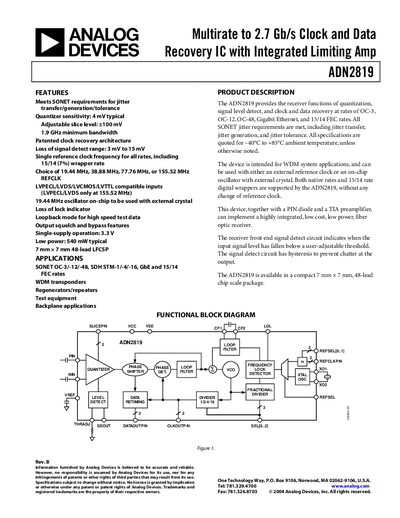
The ADN2819 is a multirate clock and data recovery IC designed for SONET/SDH, Gigabit Ethernet, and 15/14 FEC rates. It meets jitter transfer, generation, and tolerance requirements and operates from a single 3.3 V supply with low power consumption.
The device is offered in a 7 mm × 7 mm 48‑lead LFCSP package and supports selectable reference clock frequencies of 19.44 MHz, 38.88 MHz, 77.76 MHz, or 155.52 MHz. It includes features such as loss‑of‑signal detection, loopback test mode, output squelch, and programmable slice level adjustment.
| Supply Voltage (VCC) | 3.0 V – 3.6 V |
|---|---|
| Power Supply Current | 150 mA – 215 mA |
| Upper -3 dB Bandwidth | 19 GHz |
| Single‑Ended Output Swing | 300 mV – 600 mV |
| Differential Output Swing | 600 mV – 1.2 V |
| Input Voltage Range @ PIN or NIN (dc‑coupled) | 0 V – 1.2 V |
| Reference Clock Frequency Options | 19.44 MHz, 38.88 MHz, 77.76 MHz, 155.52 MHz |
The device operates from a single supply voltage between 3.0 V and 3.6 V.
Typical power consumption is about 540 mW at 3.3 V.
The ADN2819 can use 19.44 MHz, 38.88 MHz, 77.76 MHz, or 155.52 MHz reference clocks.
It is available in a 7 mm × 7 mm 48‑lead LFCSP package.