
The AD9510 is a 1.2 GHz clock distribution IC with a PLL core, dividers, delay adjust, and eight outputs. It features low phase noise, programmable dual-modulus prescaler, programmable charge pump, separate CP supply, two 1.6 GHz differential clock inputs, 8 programmable dividers, phase select for output-to-output coarse delay adjust, 4 independent 1.2 GHz LVPECL outputs, additive output jitter of 225 fs rms, 4 independent 800 MHz/250 MHz LVDS/CMOS clock outputs, additive output jitter of 275 fs rms, fine delay adjust on 2 LVDS/CMOS outputs, and a serial control port. The AD9510 is suitable for low jitter, low phase noise clock distribution and high-speed ADCs, DACs, DDSs, DDCs, DUCs, MxFEs, and other applications.
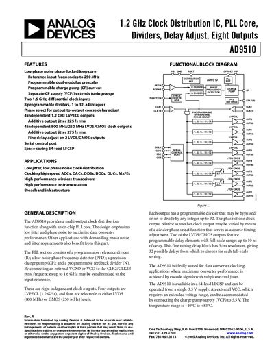
The AD9510 provides a multi‑output clock distribution function together with an on‑chip PLL core. It offers eight independent outputs—four LVPECL (1.2 GHz) and four selectable LVDS (800 MHz) or CMOS (250 MHz)—with programmable dividers and fine‑delay adjustment for sub‑nanosecond timing control. The device is supplied from a single 3.3 V rail, with an optional charge‑pump supply up to 5.5 V for external VCOs, and operates over –40 °C to +85 °C.
Typical applications include clocking high‑speed data converters, wireless transceivers, instrumentation, and broadband infrastructure where low phase‑noise and jitter are critical. The part is offered in a 64‑lead LFCSP package and is supported by an evaluation board for rapid prototyping.
| Reference Input Frequency (REFIN) | 250 MHz |
|---|---|
| LVPECL Output Frequency | 1200 MHz |
| Additive Output Jitter (LVPECL) | 225 fs rms |
| Supply Voltage | 3.3 V (single) – VCP up to 5.5 V |
| Operating Temperature Range | –40 °C to +85 °C |
The AD9510 provides eight independent clock outputs—four LVPECL and four selectable LVDS or CMOS.
The reference inputs accept frequencies up to 250 MHz.
It operates from a single 3.3 V supply, with an optional charge‑pump supply (VCP) that can be raised to 5.5 V for external VCOs.