
ADN2811 Rev. B is an OC-48/OC-48 FEC Clock and Data Recovery IC with Integrated Limiting Amp launched by Analog Devices. It meets SONET requirements.
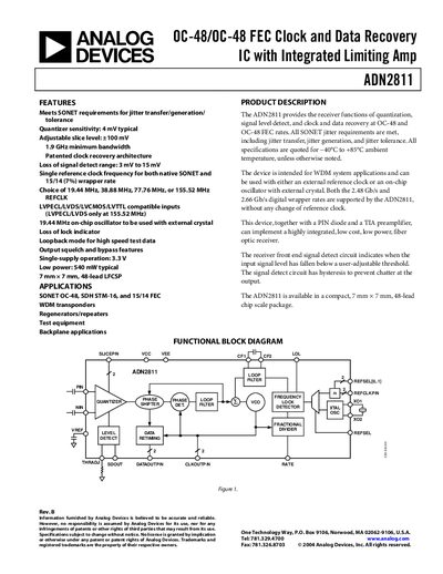
The ADN2811 is a 48‑lead LFCSP IC that provides quantization, signal‑level detection, and clock‑and‑data recovery for SONET OC‑48 and OC‑48 FEC rates. It meets SONET jitter requirements, offers selectable reference clocks, and operates from a single 3.3 V supply with low power consumption.
The document includes detailed electrical specifications, absolute maximum ratings, pin configuration, functional block diagrams, and ordering information. It also covers application notes such as loss‑of‑signal detection, loss‑of‑lock indication, and test modes like bypass and loopback.
| Input Voltage Range (DC‑Coupled) | 0 – 1.2 V |
|---|---|
| Upper –3 dB Bandwidth | 19 GHz |
| Power Supply Voltage | 3.0 – 3.6 V (typical 3.3 V) |
| Power Supply Current | 150 – 215 mA (typical 164 mA) |
| Single‑Ended Output Swing (Vse) | 300 – 600 mV |
| Package | 7 mm × 7 mm, 48‑lead LFCSP |
The device operates from –40 °C to +85 °C.
The ADN2811 supports 19.44 MHz, 38.88 MHz, 77.76 MHz, or 155.52 MHz reference clocks.
Loss of lock is indicated by the LVTTL active‑high pin LOL (Loss of Lock Indicator).
Typical power consumption is 540 mW.