
FQT2P25 is a 250V P-Channel MOSFET produced using Fairchild's proprietary DMOS technology. This device features low on-state resistance, superior switching performance, and high energy pulse withstand capability, making it well suited for high efficiency switching DC/DC converters.
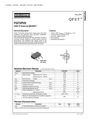
The FQT2P25 is a 250 V P‑Channel enhancement mode power MOSFET built with Fairchild's planar stripe DMOS technology. It is optimized for low on‑state resistance, fast switching, and high‑energy pulse handling, making it suitable for efficient DC/DC converter designs.
The datasheet provides absolute maximum ratings, detailed electrical characteristics, typical performance curves, and test circuit diagrams. Package information (SOT‑223) and thermal specifications are also included, along with trademark and product status notices.
| Drain‑Source Voltage (VDS) | -250 V |
|---|---|
| Continuous Drain Current (ID) @ 25 °C | -0.55 A |
| Continuous Drain Current (ID) @ 100 °C | -0.35 A |
| Pulsed Drain Current (ID) (max) | -2.2 A |
| Gate‑Source Voltage (VGS) | +30 V |
| Power Dissipation (PD) @ 25 °C | 25 W |
| Thermal Resistance, Junction‑to‑Ambient (RθJA) | 50 °C/W |
| Operating Temperature Range | -55 °C to +150 °C |
| Typical Gate Charge (Qg) | 6.5 nC |
| Output Capacitance (Coss) | 55 pF |
| Reverse Transfer Capacitance (Crss) | 8.5 pF |
| Turn‑On Delay Time | 25 ns |
| Turn‑On Rise Time | 90 ns |
| Turn‑Off Delay Time | 35 ns |
| Turn‑Off Fall Time | 60 ns |
| Package Type | SOT‑223 |
The FQT2P25 is rated for a maximum drain‑source voltage of -250 V.
It can conduct a continuous drain current of -0.55 A at 25 °C.
The typical total gate charge is 6.5 nC.
The MOSFET is supplied in an SOT‑223 surface‑mount package.