
FQT5P10 is a P-channel MOSFET produced by Fairchild. Its features include low on-state resistance, high efficiency switching performance and high energy pulse tolerance. Suitable for low voltage applications such as audio amplifiers, high efficiency switching DC/DC converters and DC motor control
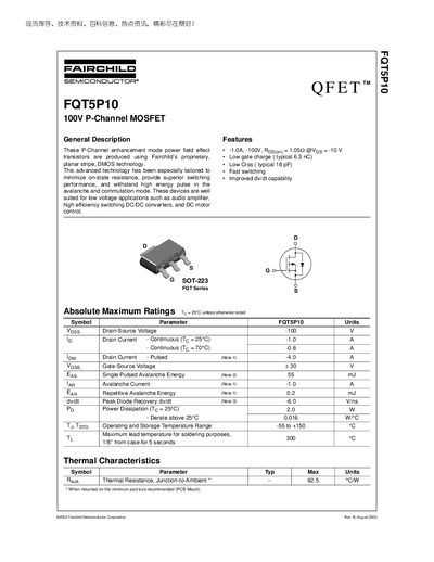
The FQT5P10 is a P‑Channel enhancement mode power MOSFET built with Fairchild’s planar stripe DMOS technology. It is intended for low‑voltage applications such as audio amplifiers, high‑efficiency DC/DC converters and DC motor control.
Key specifications include a -100 V drain‑source rating, -1 A continuous drain current at 25 °C, low on‑resistance of 1.052 Ω at VGS = ‑10 V, typical gate charge of 6.3 nC, and fast switching times (turn‑on delay ~30 ns). The device operates from –55 °C to +150 °C and has a thermal resistance of 62.5 °C/W.
| Drain‑Source Voltage (V_DSS) | -100 V |
|---|---|
| Continuous Drain Current (I_D) at 25 °C | -1.0 A |
| Pulsed Drain Current (I_D) (Note 1) | -4.0 A |
| Gate‑Source Voltage (V_GS) | +30 V |
| On‑Resistance (R_DS(on)) | 1.052 Ω @ V_GS = -10 V |
| Typical Gate Charge (Q_g) | 6.3 nC |
| Reverse Transfer Capacitance (C_rss) | 18 pF (typical) |
| Power Dissipation (P_D) at 25 °C | 2.0 W |
| Operating Temperature Range | -55 °C to +150 °C |
| Thermal Resistance, Junction‑to‑Ambient | 62.5 °C/W |
The device is rated for a maximum drain‑source voltage of –100 V.
It can conduct up to –1.0 A continuously at a junction temperature of 25 °C.
The typical total gate charge is 6.3 nC.
The on‑resistance is 1.052 Ω when V_GS = –10 V.