
This document describes the features of the FQP7N65C/FQPF7N65C 650V N-Channel MOSFET. It is produced using Fairchild's proprietary planar stripe DMOS technology, which minimizes on-state resistance, provides superior switching performance, and withstands high energy pulse in avalanche and commutation mode. These devices are suitable for high efficiency switched mode power supplies, active power factor correction, and electronic lamp ballasts based on half bridge topology.
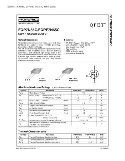
The FQP7N65C and FQPF7N65C are N‑Channel enhancement mode power MOSFETs fabricated with Fairchild’s planar stripe DMOS technology. They are designed for high‑efficiency switched‑mode power supplies, active power factor correction, and half‑bridge lamp ballast applications.\n\nThe document lists absolute maximum ratings, electrical characteristics, typical performance curves, and package dimensions for the TO‑220 and TO‑220F variants. Test circuit diagrams for gate charge, switching, and diode recovery are also included.
| Drain‑Source Voltage (V_DSS) | 650 V |
|---|---|
| Continuous Drain Current (I_D) at 25 °C | 7 A |
| Continuous Drain Current (I_D) at 100 °C | 4.2 A |
| Pulsed Drain Current (I_D) (Note 1) | 28 A |
| Gate‑Source Voltage (V_GS) | +30 V |
The maximum drain‑source voltage is 650 V.
It can conduct up to 7 A continuously at 25 °C.
No, Fairchild states the products are not authorized for use as critical components in life‑support devices.