
The document contains information about inventory, technical data, encyclopedia information, and hot news. It also discusses the features and characteristics of QFET products.
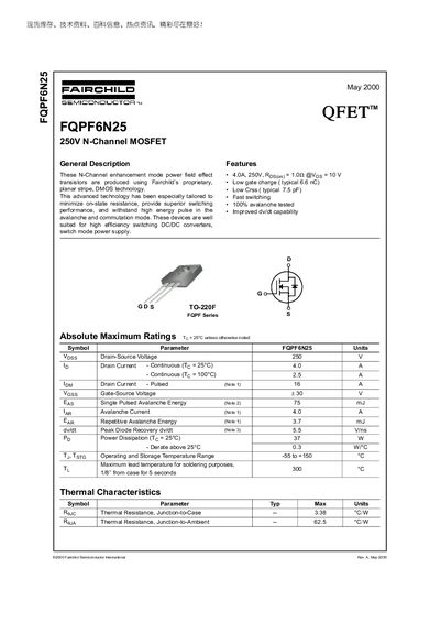
The FQPF6N25 is a 250 V N‑Channel enhancement mode power MOSFET designed for high‑efficiency switching applications such as DC/DC converters and switch‑mode power supplies. It features low gate charge, low output capacitance, fast switching, and 100 % avalanche testing.
The document lists absolute maximum ratings, electrical characteristics, typical performance curves, test circuit waveforms, and package dimensions (TO‑220F). It also includes trademark, disclaimer, and product‑status information from Fairchild Semiconductor.
| Drain‑Source Voltage (V_DSS) | 250 V |
|---|---|
| Continuous Drain Current (I_D) at 25 °C | 4.0 A |
| Pulsed Drain Current (I_D) (Note 1) | 16 A |
| Gate‑Source Voltage (V_GS) | +30 V |
| Power Dissipation (P_D) at 25 °C | 37 W |
| Junction‑to‑Case Thermal Resistance | 3.38 °C·W |
| Junction‑to‑Ambient Thermal Resistance | 62.5 °C·W |
| Typical Gate Charge (Q_G) | 6.6 nC |
| Package Type | TO‑220F |
The device is rated for a maximum drain‑source voltage of 250 V.
It can conduct up to 4.0 A continuously at a case temperature of 25 °C.
The typical gate charge is 6.6 nC.
The MOSFET is supplied in a TO‑220F package.