
FQAF17P10 is a 100V P-Channel MOSFET produced by Fairchild. It has low gate charge, low Crss, fast switching, 100% avalanche tested, improved dv/dt capability, and 175°C maximum junction temperature rating.
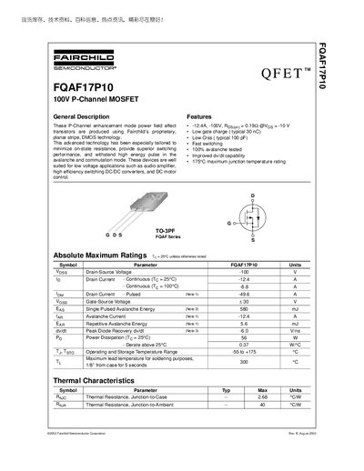
The FQAF17P10 is a P‑Channel enhancement‑mode power MOSFET built with Fairchild’s planar stripe DMOS technology. It is optimized for low on‑state resistance, fast switching, and high‑energy pulse capability, making it suitable for audio amplifiers, high‑efficiency DC‑DC converters, and DC motor control.
Key specifications include a -100 V drain‑source rating, -12.4 A continuous drain current at 25 °C, -49.6 A pulsed current, typical on‑resistance of 0.192 Ω at Vgs = ‑10 V, and a maximum junction temperature of 175 °C. The device is supplied in a TO‑3PF package with thermal resistance RθJC of 2.68 °C/W.
| Drain‑Source Voltage (VDS) | -100 V |
|---|---|
| Continuous Drain Current (ID) at 25 °C | -12.4 A |
| Pulsed Drain Current (ID,pulse) | -49.6 A |
| Gate‑Source Voltage (VGS) | +30 V |
| On‑Resistance (RDS(on)) typical | 0.192 Ω @ VGS = -10 V |
| Typical Gate Charge (Qg) | 30 nC |
| Reverse Transfer Capacitance (Crss) typical | 100 pF |
| Maximum Junction Temperature (Tj) | 175 °C |
| Thermal Resistance Junction‑to‑Case (RθJC) | 2.68 °C/W |
| Package | TO‑3PF |
The device is rated for a maximum drain‑source voltage of -100 V.
It can handle a continuous drain current of -12.4 A at 25 °C.
The MOSFET is supplied in a TO‑3PF package.
The typical total gate charge is 30 nC.