
This manual introduces the basic concepts and usage methods of QFET devices, including device structure, characteristics, applications and parameter selection.
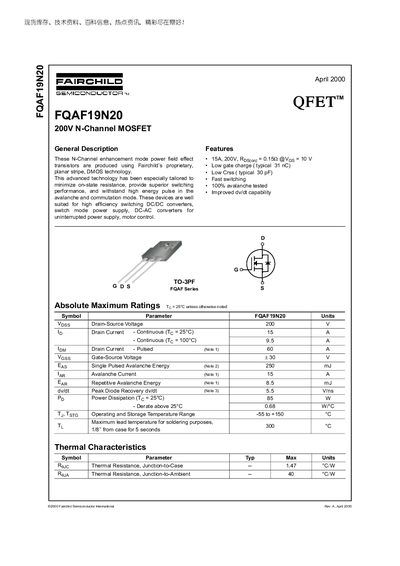
The FQAF19N20 is a 200 V N‑Channel enhancement‑mode power MOSFET built with Fairchild’s planar‑stripe DMOS technology. It offers low on‑resistance, fast switching, and high avalanche capability, making it suitable for DC‑DC converters, SMPS, motor control and UPS applications.
The document provides absolute maximum ratings, thermal characteristics, electrical parameters, typical performance curves, and package dimensions for the TO‑3PF package, along with trademark and disclaimer information.
| Drain‑Source Voltage (VDS) | 200 V |
|---|---|
| Continuous Drain Current (ID) @ 25 °C | 15 A |
| Continuous Drain Current (ID) @ 100 °C | 9.5 A |
| Pulsed Drain Current (ID) (Note 1) | 60 A |
| Gate‑Source Voltage (VGS) | +30 V |
| Power Dissipation (PD) @ 25 °C | 85 W |
| Junction‑to‑Case Thermal Resistance (RθJC) | 1.47 °C·W |
| Junction‑to‑Ambient Thermal Resistance (RθJA) | 40 °C·W |
| On‑Resistance (RDS(on)) typical | 0.12‑0.15 Ω |
| Total Gate Charge (Qg) typical | 31 nC |
The device can conduct a continuous drain current of 15 A at 25 °C.
The typical total gate charge is 31 nC.
The MOSFET is rated for a drain‑source voltage of 200 V.
The part can dissipate up to 85 W when the case temperature is 25 °C.