
FQAF17P10 is a P-Channel enhancement mode power field effect transistor with low on-state resistance, superior switching performance, and high energy pulse withstand capability. It is well suited for low voltage applications such as audio amplifier, high efficiency switching DC/DC converters, and DC motor control.
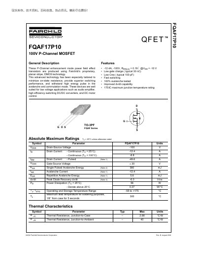
The FQAF17P10 is a P‑Channel enhancement mode power MOSFET produced using Fairchild’s proprietary planar‑stripe DMOS technology. It is optimized for low on‑resistance and fast switching, making it suitable for low‑voltage applications such as audio amplifiers, high‑efficiency DC/DC converters and DC motor control.
Key electrical characteristics include a drain‑source breakdown voltage of –100 V, continuous drain current of –12.4 A at 25 °C, typical on‑resistance of 0.19 Ω at VGS = –10 V, total gate charge of about 30 nC, and a maximum junction temperature of 175 °C. The device is supplied in a TO‑3PF package with defined thermal resistance values. This manual is written in Chinese.
| Drain‑Source Voltage (VDS) | -100 V |
|---|---|
| Gate‑Source Voltage (VGS) | ±30 V |
| On‑Resistance (RDS(on)) @ VGS = –10 V | 0.19 Ω (typical) |
| Output Capacitance (Coss) | 310‑400 pF (typical) |
| Reverse Transfer Capacitance (Crss) | 100‑130 pF (typical) |
| Power Dissipation (PD) @ 25 °C | 56 W |
| Maximum Junction Temperature (TJ) | 175 °C |
| Thermal Resistance Junction‑to‑Case (RθJC) | 2.68 °C/W |
The device can withstand a drain‑source voltage of –100 V.
Typical RDS(on) is 0.19 Ω at VGS = –10 V.