
This document is a PDF datasheet of QFET, which details the basic parameters and performance characteristics of QFET.
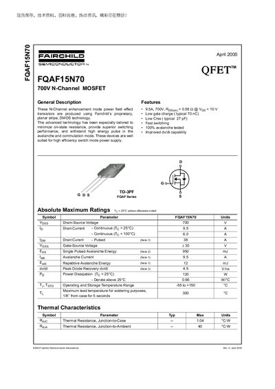
The FQAF15N70 is a 700 V N‑Channel enhancement mode power MOSFET built with Fairchild's planar stripe DMOS technology. It is designed for high‑efficiency switch‑mode power supplies, offering low on‑state resistance and fast switching performance.
The document includes absolute maximum ratings, detailed electrical characteristics, typical performance curves, and test circuit diagrams. Package dimensions for the TO‑3PF case and trademark information are also provided.
| Drain‑Source Voltage (VDS) | 700 V |
|---|---|
| Continuous Drain Current (ID) @ 25°C | 9.5 A |
| Pulsed Drain Current (ID) (Note 1) | 38 A |
| Typical Gate Charge (Qg) | 70 nC |
| Input Capacitance (Ciss) typical | 2790 pF |
| On‑Resistance (RDS(on)) @ VGS=10 V | 0.56 Ω |
| Power Dissipation (PD) @ 25°C | 120 W |
| Thermal Resistance Junction‑to‑Case (RθJC) | 1.04 °C/W |
| Thermal Resistance Junction‑to‑Ambient (RθJA) | 40 °C/W |
The maximum drain‑source voltage is 700 V.
It can handle a continuous drain current of 9.5 A at 25 °C.
The typical gate charge is 70 nC.
The on‑resistance is approximately 0.56 Ω at VGS=10 V.